MSP430 Microcontroller using ADC and PWM
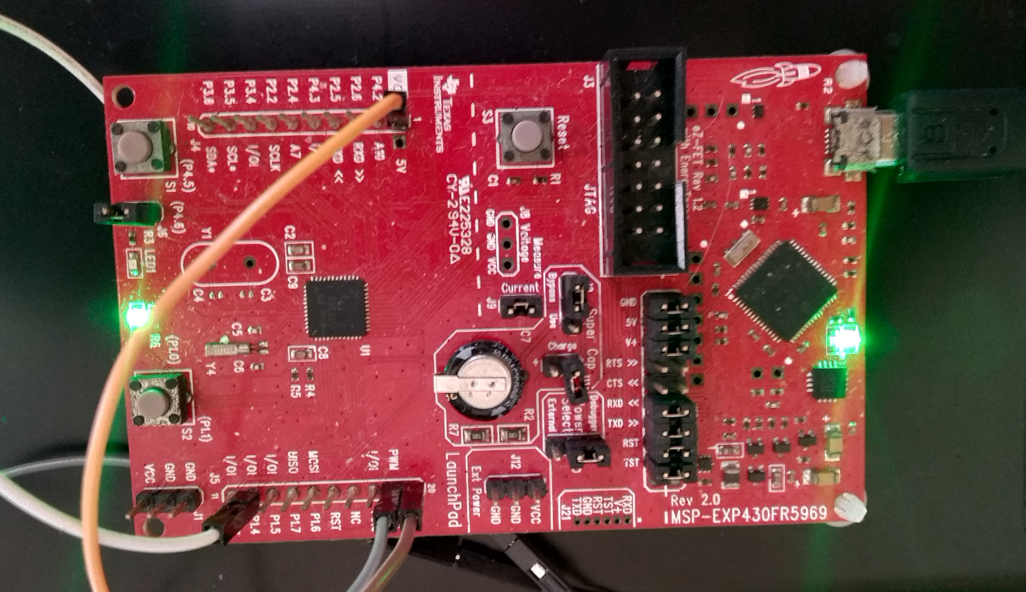
It is a simple project using PWM as output and ADC as input in a MSP430FR5969 Microcontroller, in other words, the output voltage (for example a LED) can increase/decrease according to the ADC Value.
The MSP430FR5969 DataSheet and User’s Guide that is used to develop this code. You can find this code here.
Code
CLOCK
As you can see in the datasheet, you can configure different clocks for different utilities, so you can configure the clocks as your project needs. in this case, the MCLK -> DCO = 1MHZ, the ACLK -> LFXTCLK (~32Khz) = 32.768 Hz and the SMCLK -> DCO (1Mhz / 32) = 31.250 hz
// CLOCK

  // MASTER CLOCK (MCLK)                    // CPU CLOCK
  CSCTL0_H = CSKEY >> 8;                    // Unlock CS registers
  CSCTL1 = DCOFSEL_0;                       // DCO = 1Mhz
  CSCTL2 = SELM__DCOCLK;                    // MCLK -> DCO
  CSCTL3 = DIVM__1;                         // Div / 1 (therefore the MCLK clock remains the same)

  // AUXILIARY CLOCK (ACLK)                 // TIMER CLOCK
  CSCTL2 |= SELA__LFXTCLK;                  // ACLK -> LFXTCLK (~32Khz) = 32.768 Hz
  CSCTL3 |= DIVA__1;                        // Div / 1

  // SUB-MASTER CLOCK (SMCLK)                // ADC CLOCK
  CSCTL2 |= SELS__DCOCLK;                    // SMCLK -> DCO
  CSCTL3 |= DIVS__32;                        // Div /32 (1Mhz / 32) = 31.250 hz
PWM
This example project uses the TimerB counter with the Up-Mode, and Reset/set mode. The output is reseted when the timer counts to TBxCCR1 value, and it is set when the timer counts to the TBxCCR0 value, so hence it’s clear that if the relation TBxCCR0/TBxCCR1 changes, the duty cycle PWM will also change.
  // Configure PWM output (TIMER B)
  TB0CTL = TBSSEL__ACLK | ID__1 | MC__UP | TBCLR | TBIE;             // TIMERB -> ACLK , DIV/1 , UP_MODE, Interrupt Enable
  TB0CCTL1 = OUTMOD_7;                                               // MODE RESET/SET

  //Duty Cycle
  TB0CCR0 = 1000-1;
  TB0CCR1 = 100;                                                    // Duty Cycle = (10%) - initial duty cycle
Initialization ADC function:
It’s a 12-bit resolution ADC, therefore N=2^12= 4.096, so the LSB = 3.45v/4096 = 0.0008423 = 0.84mv difference for each bit. as ADC12VRSEL = 0, Therefore VR+ = AVCC (3.45v) and VR-= AVss (0v).
  // Configure ADC12

  ADC12CTL0 &= (ADC12ENC);										   //  Conversion Disabled for now
  ADC12CTL0 = ADC12SHT0_2 | ADC12ON;                               //  Sampling time (16 cycles) and Turn on the ADC
  ADC12CTL1 = ADC12SSEL_3 | ADC12SHP;                              //  ADC12CLK -> SMCLK
  ADC12CTL2 = ADC12RES__12BIT;                                     //  12-bit resolution
  ADC12MCTL0 = ADC12INCH_2 | ADC12DIF;                             //  Channel2 ADC input select; Vref=AVCC
  ADC12IER0 = ADC12IE0;                                            //  Enable ADC conv complete interrupt
Read ADC value and change the output
ADC12MEM0 is the register that holds the ADC Value.
while (1)
  {
    __delay_cycles(5000);
    ADC12CTL0 |= ADC12ENC | ADC12SC;                               // Start sampling/conversion
	//while (!(ADC12IFGR0));                                       // Wait the ADC time sampling

    __bis_SR_register(GIE);                                        // Interrupt Enable
    __no_operation();                                              // For debugger
  }
}

// ADC12 INTERRUPT
#pragma vector = ADC12_VECTOR
__interrupt void ADC12_ISR(void){

    P1OUT ^= BIT0;                                                   // Output Led to verify if the ADC interrupt is OK

    result = ADC12MEM0;
    if(result>=0x0340 && result < 0x0A80){                     //  ADC >= 822 AND ADC < 2688
        TB0CCR1 = 450;                  //   PWM Duty Cycle (45%)
    }
    else if(result>=0x0A80){                                      // ADC > = 2688
        TB0CCR1 = 900;                  //   PWM Duty Cycle (90%)
    }
    else{
        TB0CCR1 = 100;                  //   PWM Duty Cycle (10%)
}

}

//TIMER B INTERRUPT (B1 VECTOR)
#pragma vector=TIMER0_B1_VECTOR
__interrupt void Timer_B1(void){

    TB0CTL &= ~(TBIFG);                                               // Clear Flag

}